
Transforming organizations, driving value 


Mirafra Software Technologies Pvt Ltd is ISO 9001:2015 (Quality Management System) and ISO 27001:2022 (Information Security Management System) certified Company.
Who we are
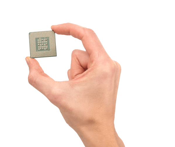
From architecture to implementation and silicon, from chip bring-up to post silicon validation, from embedded software to digital software, Mirafra offers end-to-end capabilities in SoC chip design, entire software stack development honed over two decades of rich experiences.
From advanced application development to data analytics, machine learning, and artificial intelligence, Our services are built on a foundation of innovation.
Our services

Mirafra has provided excellent Individuals to execute the RTL, DV and PD of blocks at various stages. Mirafra is very proactive in understanding the needs of customer and provides the contractors at various levels of experience. Also, Mirafra monitors the progress of the individuals provided to Achronix and takes corrective steps as required.
V. Mohan Krishna Director, HW Engineering, Bangalore.
Working with Mirafra has been a fantastic experience. Their communication was
top-notch, and the active engagement on Jira ensured a transparent and efficient
workflow. The working relationship was excellent, contributing to an
exceptionally smooth project. Mirafra's ability to read between the lines of the
spec showcased their attention to detail, and their flexibility as a team was truly
impressive.
The initiative they took in creating their own verification testbench
demonstrated their commitment to delivering a high-quality solution. The in-
depth knowledge transfer provided added value, fostering trust and a positive
underlying culture. Highly recommend their professional and adaptable
approach
From an Automotive client
“I am extremely pleased with the consistent and invaluable support provided by
the Mirafra team over the past year and a half. Their dedication to our 3D
Performance at Fixed Frequency client integrated graphics projects and
AMX/ALPS Si calibration/correlation activities has played a pivotal role in the
success of these initiatives. The level of expertise and commitment
demonstrated by Mirafra has empowered our team to take the lead in these
challenging projects. I extend my sincere gratitude for the outstanding support
thus far and look forward to maintaining this positive momentum as we venture
into upcoming projects.
Absolutely, today marks the completion of our assignment with the Mirafra team.
I want to express my sincere gratitude for their invaluable contribution to our
project, adding significant value to our product. Working with Mirafra has been a
pleasure, and I appreciate their dedication and expertise throughout the
collaboration. I look forward to the possibility of future collaborations and
extending my thanks for a job well done!”
From a CPU market leader
The best part of working with Mirafra is the process is that continuously improving. Mirafra frequently reaches out to get feedback. The feedback is quickly used to tailor the processes to ensure the best talent is hired. Mirafra puts prospective candidates through an internal screening processes to ensure we get to interview the best candidates. There is an ongoing feedback on the job description - must haves and good to haves with the hiring team. This ensures we cast a wide net but also get appropriate candidates applying for the role. Mirafra follows up post interview to ensure the hiring process is successfully completed.
Almost all of my team's external members are from Mirafra. These team members are some of the most productive and innovative team members. We continue to repose faith on Mirafra to continue bringing in the best talent for Mirafra.
Harsha TalkaduNijagunaswamy Senior Manager, Infineon India

Senior Manager /Asst. Director – Sales
Location: Bangalore
Job Description:
Job Requirement:
Experience (years) : 12+ years
Education Qualification:
PSV Characterization
Location: Bangalore
Job Description:
Experience (years) : 3-6 years
Education Qualification:
BTECH/MTECH in Electrical/Electronics/Computer Science Engineering or Equivalent
C++ Developer
Location: Hyderabad
Job Description:
Experience (years) : 2 - 4 Years
Education Qualification:
BTECH/MTECH in Electrical/Electronics/Computer Science Engineering or Equivalent
Database management
Location: Hyderabad
Job Description:
Experience (years) : 5+ years
Education Qualification:
BTECH/MTECH in Electrical/Electronics/Computer Science Engineering or Equivalent
HPC SOFTWARE ENGINEER
Location: Bangalore
Job Description:
Job Requirement:
Experience (years) : 4-10 Years
Education Qualification:
BTECH/MTECH in Electrical/Electronics/Computer Science Engineering or Equivalent
Synthesis Engineer
Location: India (Hybrid/Onsite)
Job Description:
Experience (years) : 2+ years
Education Qualification:
BTECH/MTECH in Electrical/Electronics/Computer Science Engineering or Equivalent
Physical Design Engineer
Location: Bangalore / Noida
Job Description:
Experience (years) : 4+ years
Education Qualification:
BTech/ MTech Electrical/Electronics/Computer Science Engineering or Equivalent.
Formal Verification
Location: Hyderabad
Job Description:
Job Requirement:
Experience (years) : 4-10 yrs
Education Qualification:
BTECH/MTECH in Electrical/Electronics/Computer Science Engineering or Equivalent
FPGA Engineer
Location: Hyderabad
Job Description:
Experience (years) : 3-6 years
Education Qualification:
BTECH/MTECH in Electrical/Electronics/Computer Science Engineering or Equivalent
Design Verification(Ethernet/Wifi/BT)
Location: Pune
Job Description:
Experience (years) : 4+ years
Education Qualification:
BTECH/MTECH in Electrical/Electronics/Computer Science Engineering or Equivalent
Design Verification(High Speed Protocol)
Location: Bangalore
Job Description:
Experience (years) : 4+ years
Education Qualification:
BTECH/MTECH in Electrical/Electronics/Computer Science Engineering or Equivalent
Design Verification (Cache)
Location: Bangalore
Job Description:
Experience (years) : 4+ years
Education Qualification:
BE/ME
Design Verification(SOC)
Location: Bangalore
Job Description:
Job Requirement:
Proven understanding of digital hardware verification language Verilog/System Verilog HDL.
Experience (years) : 5+ years
Education Qualification:
BE/ME
Design Verification(GLS)
Location: Bangalore
Job Description:
Experience (years) : 4+ years
Education Qualification:
BE/ME
Design Verification Engineer
Location: Noida
Job Description:
• SOC Verification engineers with 3+ years of experience
• Knowledge of ARM architecture, CPU fundamentals & Cache coherency
• Experience with C/C++, assembly, and scripting languages.
• Familiarity with low-power design and verification
• Develop CDV UVM verification environments at system level
• Verify CPU connectivity to IP blocks
• Develop SoC test plans and test cases and track metrics including code and functional covera
Job Requirement:
• Bachelor’s or Master’s in EE/CS or related field
• 3+ years of SoC in ASIC/FPGA verification experience
• Proficiency in SV and UVM
• Experience with simulation, emulation, and formal verification
• Strong debugging and problem-solving skills
Experience (years) : 3+ years
Education Qualification:
BTECH/MTECH in Electrical/Electronics/Computer Science Engineering or Equivalent
Analog Layout
Location: Bangalore / Hyderabad
Job Description:
Job Requirement:
TSMC 2nm or 3 nm
Experience (years) : 4-8 years
Education Qualification:
BTech
Analog Circuit Design
Location: Bangalore / Hyderabad
Job Description:
Experience (years) : 5-9 years
Education Qualification:
BTECH/MTECH in Electrical/Electronics/Computer Science Engineering or Equivalent
IO Layout
Location: Bangalore
Job Description:
Experience (years) : 4-9 years
Education Qualification:
BTECH/MTECH in Electrical/Electronics/Computer Science Engineering or Equivalent
Memory Layout
Location: Bangalore
Job Description:
Job Requirement:
Experience (years) : 5-7 years
STA
Location: Bangalore / Noida
Job Description:
Experience (years) : 3+ years
Education Qualification:
BTECH/MTECH in Electrical/Electronics/Computer Science Engineering or Equivalent
DFT Engineer
Location: India (Hybrid/Onsite)
Job Description:
Experience (years) : 4+ years
Education Qualification:
BTECH/MTECH in Electrical/Electronics/Computer Science Engineering or Equivalent
AMS Verification
Location: Bangalore / Hyderabad
Job Description:
Experience (years) : 3+ years
Education Qualification:
BTECH/MTECH in Electrical/Electronics/Computer Science Engineering or Equivalent
Design Verification Engineer
Location: Hyderabad
Job Description:
Job Requirement:
•Processor / PCI / DDR / Memory/C/C++
Experience (years) : 5-15 years
Education Qualification:
BE / ME
Design Verification Engineer
Location: Bangalore
Job Description:
Job Requirement:
• Bachelor’s or Master’s in EE/CS or related field
• 5+ years of SoC in ASIC/FPGA verification experience
• Proficiency in SV and UVM
• Strong debugging and problem-solving skills
Experience (years) : 5+ years
Education Qualification:
BTECH/MTECH in Electrical/Electronics/Computer Science Engineering or Equivalent
ATE Engineer
Location: Bangalore
Job Description:
Job Requirement:
Experience (years) : 3-10 years
Education Qualification:
BTECH/MTECH in Electrical/Electronics/Computer Science Engineering or Equivalent
Functional Validation
Location: Hyderabad/ Chennai
Job Description:
Experience (years) : 4-10 years
Education Qualification:
BTECH/MTECH in Electrical/Electronics/Computer Science Engineering or Equivalent
RTL ASIC SoC Architect / Lead RTL Design Engineer
Location: India (Hybrid/Onsite)
Job Description:
• System & Micro-Architecture Definition: Proven ability to translate product requirements and specifications into scalable, power- and performance-optimized micro-architectures.
• SoC Integration & Sub-System Ownership: Extensive experience in top-level SoC integration, clock/reset architecture, power domain planning, and cross-IP coordination.
• Bus Protocols & Interconnects: Strong expertise in industry-standard protocols such as AXI/AHB/APB, coherent interconnects (ACE/CHI preferred), and peripherals including PCIe, USB, Ethernet, CXL, and DDR.
• CPU & Memory Subsystems: Hands-on experience with CPU subsystem integration (ARM/ARC/RISC-V), cache hierarchy, MMU, and memory controller architectures (DDR, LPDDR).
• Low-Power Architecture: Deep understanding of low-power techniques including UPF/CPF, power gating, clock gating, DVFS, multi-voltage designs, and retention strategies.
• RTL Design & Coding Practices: Strong SystemVerilog RTL coding skills with emphasis on reuse, configurability, and synthesis-friendly design.
• Verification & Quality Sign-off: Ability to review and guide verification strategy, static checks test plans, functional coverage, assertions, and regression quality metrics.
• Synthesis, STA & Sign-off: Expertise in synthesis (Design Compiler), static timing analysis, timing closure across multiple PVT corners, and ECO handling.
• Formal & Equivalence Checking: Strong experience with formal verification and logical equivalence checking (LEC).
• DFT & Debug: Good working knowledge of DFT architectures (scan, MBIST, JTAG) and debug/trace infrastructures.
• Post-Silicon Bring-up: Experience with silicon bring-up, lab debugging, silicon validation, and correlation between RTL, simulation, and silicon behavior.
• Chip IO & Packaging: Understanding of chip IO planning, pad ring integration, signal integrity considerations, and packaging constraints.
• Cross-Functional Leadership: Ability to work closely with PD, DV, DFT, firmware, and software teams to ensure seamless execution and delivery.
• Mentoring & Technical Leadership: Proven capability to mentor engineers, review designs, drive best practices, and own delivery of complex SoC programs.
Job Requirement:
• SoC & Micro-Architecture: End-to-end Consumer SoC architecture and micro-architecture design optimized for PPA and real-world use cases.
• CPU & Interconnects: Integration of ARM/ARC/RISC-V CPU subsystems, cache hierarchies, AXI/AHB/APB, and coherent interconnects.
• Memory & High-Speed Interfaces: DDR/LPDDR subsystems and consumer interfaces such as PCIe, USB, Ethernet, CXL, MIPI, and display.
• Low-Power Design: Expertise in UPF-based low-power architecture, clock/power gating, DVFS, and multi-voltage domains.
• RTL, Verification & Sign-off: Strong SystemVerilog RTL, synthesis, STA/timing closure, formal (LEC), and DV/coverage review.
• Post-Silicon & Leadership: Silicon bring-up/debug experience with strong technical leadership and cross-functional collaboration.
Experience (years) : 10+ years
Education Qualification:
BTECH/MTECH in Electrical/Electronics/Computer Science Engineering or Equivalent
Design Verification Engineers
Location: Noida
Job Description:
Job Requirement:
Experience (years) : 3+ Year
Education Qualification:
BTECH/MTECH in Electrical/Electronics/Computer Science Engineering or Equivalent
RTL Design Engineer
Location: India (Hybrid/Onsite)
Job Description:
Experience (years) : 4+ years
Education Qualification:
BE/B-Tech/ME/M-Tech degree in Electronics and Communication, Electrical Engineering, or related field
Multimedia- Video/V4L2
Location: Hyderabad
Job Description:
Job Requirement:
• Bachelors\Master’s degree in Engineering, Information Systems, Computer Science, or related field 3-5 years of experience with Programming Language such as C, C++, Java, Python.
Experience (years) : 3+ Year
Education Qualification:
BTECH/MTECH in Electrical/Electronics/Computer Science Engineering or Equivalent
Multimedia Audio DSP
Location: Hyderabad
Job Description:
Job Requirement:
Experience (years) : 3+ Year
Education Qualification:
BTECH/MTECH in Electrical/Electronics/Computer Science Engineering or Equivalent
Analog Circuit Design
Location: India (Hybrid/Onsite)
Job Description:
Skills/Experience:
Experience (years) : 2+ Year
Education Qualification:
BE/B-Tech/ME/M-Tech degree in Electronics and Communication, Electrical Engineering, or related field.
IO Layout
Location: India (Hybrid/Onsite)
Job Description:
Experience (years) : 3+ Year
Education Qualification:
BE/B-Tech/ME/M-Tech degree in Electronics and Communication, Electrical Engineering, or related field.
PMIC Characterization
Location: Bangalore, Hyderabad, Noida
Job Description:
Experience (years) : 2 - 7 years
Education Qualification:
BTECH/MTECH in Electrical/Electronics/Computer Science Engineering or Equivalent
FPGA Design Engineer
Location: Bangalore, Hyderabad, Noida
Job Description:
Experience (years) : 3 - 12 Years
Education Qualification:
BTECH/MTECH in Electrical/Electronics/Computer Science Engineering or Equivalent
Emulation Engineer
Location: Bangalore, Hyderabad, Noida
Skills/Experience:
Experience (years) : 3 - 12 Years
Education Qualification:
BTECH/MTECH in Electrical/Electronics/Computer Science Engineering or Equivalent
Physical Verification Engineer
Location: India (Hybrid/Onsite)
Job Description:
Skills/Experience:
Experience (years) : 4+ Year
Education Qualification:
B-TECH/M-TECH in Electrical/Electronics/Computer Science Engineering or Equivalent
Linux Device Driver
Location: Bangalore, Hyderabad, Chennai, Pune
Job Description:
Experience (years) : 5-10 years
Education Qualification:
BTECH/MTECH in Electrical/Electronics/Computer Science Engineering or Equivalent